
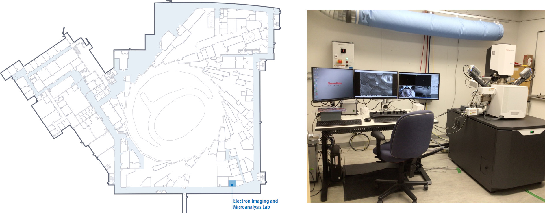
EIML - Electron Imaging & Microanalysis Lab
The Electron Imaging and Microanalysis Lab is a facility with flexibility for the analysis of any type of soft or hard materials, including in situ dynamic studies in a natural state and a range of environmental conditions (high vacuum, low vacuum and wet/humid reactive environments). The EIML permits the study and development of novel materials as well as the analyses of biological samples without the requirement of preparation methods that can or may introduce artefacts.
Applications
The only electron beamline at the CLS, the EIML supports applications including:
- Material characterization: Determining the structure and elemental composition of unknown materials.
- Materials development: Investigating the characteristics of novel materials, identifying possible causes of material failures or defects by examining structural and elemental composition.
- Elemental analysis: Identifying the elemental composition of materials and mapping their distribution within a sample.
- Process control: Monitoring structural and elemental changes during in situ experiments, or verifying sample states at different points during a synchrotron experiment.
- Geology and mineralogy: Studying the composition of rocks and minerals and tailing pond deposits to understand their formation and properties.
Techniques
Scanning Electron Microscopy
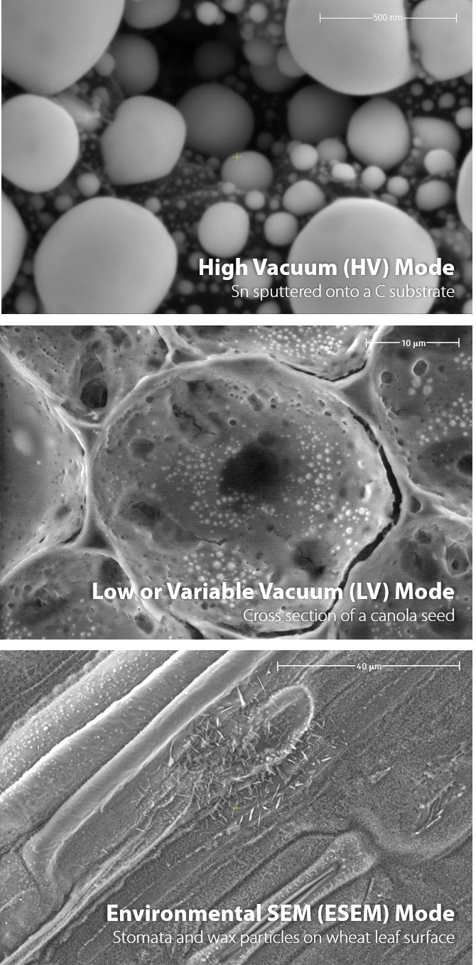
Scanning Electron Microscopy uses a focused beam of electrons incident on a sample, producing signals with information about the surface topography and composition of the sample. The electron beam is scanned in a raster scan pattern across the sample, and the resulting information is combined to produce an image. Incident or primary beam electrons interact with the atoms in the sample giving rise to secondary (SE) and backscattered electrons (BSE). Secondary electrons provide topographical information while backscattered electrons provide contrast that is driven by the atomic number of the elements present, such that the higher the atomic number the brighter the area will appear.
The Scanning Electron Microscope (SEM) at the EIML is equipped with heating stages (for high and variable vacuum conditions), STEM (STEM-in-SEM) and EDS detectors, a Quick-loader for transferring samples under controlled atmospheres from a glove-box, and equipment for MAP Mineralogy measurements, making this a uniquely versatile facility capable of complementing a wide variety of scientific applications.
With High Vacuum (HV), Low or Variable Vacuum (LV), and Environmental (ESEM) modes available, a wide range of samples, from conductive and insulators to hydrated biological specimens, can be studied.
Energy Range: 200 eV-30 keV
Applications:
CROP DEVELOPMENT ENERGY MATERIALS CATALYSTS BIOMEDICAL IMAGING OIL & GAS
Scanning Transmission Electron Microscopy (STEM-in-SEM)
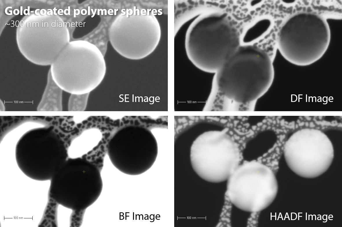
A retractable Scanning Transmission Electron Detector (STEM) in the SEM (STEM-in-SEM) allows the analysis of electron transparent specimens using low energies (max. 30keV). Images can be obtained at lower keV resulting in ultra high-resolution imaging with higher contrast. This software-based segmentation integrated detector allows Bright Field (BF), Dark Field (DF) and High Angle Annular Dark Field (HAADF) imaging and analysis to be carried out in High or Low Vacuum modes.
EDS analysis at high spatial resolutions and the analysis of biological samples (<2µm thick) is possible.
Energy Range: 200 eV-30 keV
Applications:
CROP DEVELOPMENT ENERGY MATERIALS CATALYSTS BIOMEDICAL IMAGING OIL & GAS
Energy Dispersive Spectroscopy (EDS)
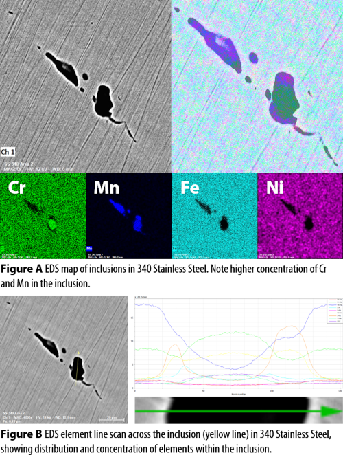
Energy Dispersive Spectroscopy is based on the interaction a beam of primary electrons and a specimen giving rise to the emission of characteristic X-rays from the atoms within the sample. Each element emits X-rays at specific energies or emission 'lines' named after the shell of initial vacancy (K, L, M, etc). These emitted X-rays are collected and analyzed using an energy-dispersive spectrometer.
The distribution of elements can be presented as element maps (Figure A) or concentrations along a line (Figure B) by acquiring spectra at each pixel. EDS analysis is mainly qualitative, but by using internal manufacturer's standards, or controlled standards, quantitative information can be obtained.
Energy Range: 200 eV-30 keV
Applications:
CROP DEVELOPMENT ENERGY MATERIALS CATALYSTS BIOMEDICAL IMAGING OIL & GAS
MAPS Mineralogy
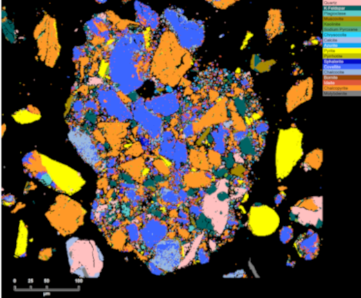
MAPS (Modular Automated Processing System) Mineralogy is a sophisticated and automated mineralogical analysis software program designed to rapidly and accurately characterize the mineral composition of ore samples and tailings, providing essential information for process optimization, resource evaluation, and metallurgical performance assessment.
Areas of interest are divided into multiple tiles, with Back-Scattered Electron images recorded in sequence and stitched together. Using two EDS detectors, spectra are obtained and compared to a database of known mineral species, creating a high-resolution mineral map.
The best-match principle used in Maps Mineralogy Software, referred to as Mixel Technology, is especially powerful and valuable for samples that contain fine-grained sub-pixel phases and boundary textures, such as: shales and mudstones, crypto-crystalline rocks, and small inclusions. The deconvolution process allows the accurate identification and quantification of sub-species in solid-solution series, including compositional zonation, and trace or minor element substitutions (such as arsenic in pyrite or iron in sphalerite). Maps Mineralogy Software automatically detects which sub-species of a solid-solution are present in the sample.
Energy Range: 200 eV-30 keV
Applications:
CROP DEVELOPMENT ENERGY MATERIALS CATALYSTS BIOMEDICAL IMAGING OIL & GAS
Specifications
| Location | Room 1082 |
| Electron Energy Range | 200eV–30keV |
| Electron Current | 1pA to 200nA |
| Resolution | <10nm (sample dependent) |
Contacts
Burke Barlow EIML Scientist
EIML Beamline Video
Access
A proposal submission is not needed for EIML-only access. The EIML may be added to a beamline proposal to support beamline data. To request access or to inquire about industry pricing please contact EIML staff.
Given the high demand for these techniques and the intensive support required to facilitate use of the EIML, a fee will be applied to all beamtime using the EIML, with variable pricing for academic and purchased access. Fees below will apply to all academic time. Pricing is subject to change. All fees will be discussed with users prior to beamtime.
Academic Pricing
Contact our Industry Services group for purchased access pricing.
Data CollectionIncludes staff and equipment costs |
$100 per hour |
Unattended Data Collection (eg. MAPS)Includes equipment costs |
$25 per hour |
Sample Preparation or Instrument SetupIncludes staff costsEither for EDS mapping or MAPS data collection or analysis of EDS and MAPS data |
$75 per hour |
User TrainingRequired for users collecting their own data |
$75 per hour |
User Data CollectionIncludes equipment costsUser collects own data. User training is required. |
$50 per hour |